Printed circuit board deconstruction techniques
Hits: 1042
Release time: 2022-06-20 10:29:54
The primary purpose of printed circuit board (PCB) reverse engineering is to determine electronic system or subsystem functionality by analyzing how components are interconnected. with a goal of removing exterior coatings and accessing individual PCB layers

Figure 1: Separated layers of the Emic 2 Text-to-Speech Module, a 4-layer PCB. On their own, the layers only tell part, if any, of the story. Placed together, a complete circuit layout can be identified.
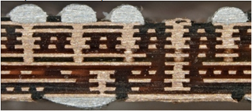
Figure 2: Cross-section of Apple’s 10-layer iPhone 4 Logic Board [8]. Inter-layer spacing is approximately 2mil and total thickness is only 29.5mil (0.75mm).
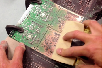
Figure 3: Hand sanding of a PCB to remove solder mask.
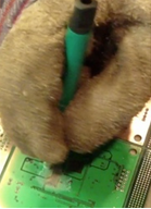
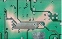
Figure 5: Using a fiberglass scratch brush on a PCB (left). The area of solder mask (1.1” x 0.37”) was removed in under one minute (right).
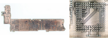
Figure 4: iPhone 4 Logic Board with solder mask removed (left). A 235x magnification shows all copper traces intact with minimal scratching (right).
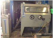
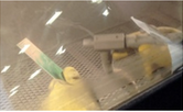
Figure 6: The TP Tools Skat Blast 1536 Champion abrasive blast cabinet (left) and interior view showing a target PCB and ideal positioning of the nozzle (right).
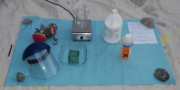
Figure 8: Workspace for our chemical removal experiments.

Figure 7: Top side of a PCB after abrasive blasting (left). A 235x magnification (right) shows the pitting on the PCB surface in more detail.

Figure 9: Results with Ristoff C-8 after a 30 minute (left), 60 minute (center), and 90 minute (right) soak at 130°F.
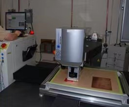
Figure 11: The LPKF MicroLine 600D UV Laser System.
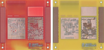
Figure 10: Results with Magnastrip 500 after a 60 minute (left) and 75 minute (right) soak at 150°F.

Figure 12: Small areas of solder mask (1.22" x 0.12") removed via laser ablation.

Figure 14: Using the Dremel tool to expose layer 3 through the substrate (left) and the resulting inner layer (right).
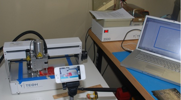
Figure 15: The T-Tech QuickCircuit 5000 PCB Prototyping System and host laptop running IsoPro 2.7.
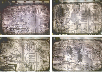
Figure 17: Inner layers 2 through 5 of a portion of the iPhone 4 Logic Board (clockwise starting at the upper left) achieved with CNC milling.
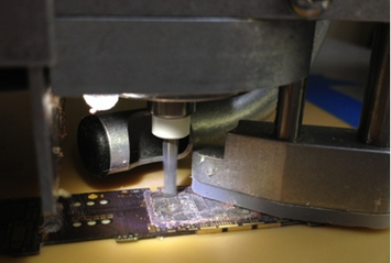
Figure 16: Close-up of the T-Tech QuickCircuit 5000 milling a layer of the iPhone 4 Logic Board.
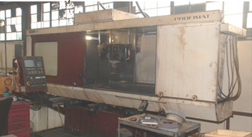
Figure 18: The Blohm PROFIMAT CNC Creep Feed Surface Grinder with a Siemens SINUMERIK 810G controller.
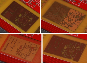
Figure 19: Inner layers 2 through 5 of a 6- layer PCB achieved with surface grinding (clockwise starting from the upper left).
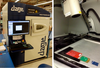
Figure 20: The DAGE XD7500VR X-ray System (left) and inside the X-ray chamber (right).
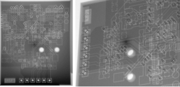
Figure 21: X-ray images of a 4-layer PCB, top down (left) and angled close-up (right).
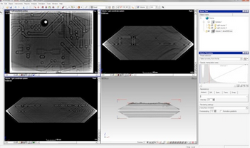
Figure 22: Screenshot from VGStudio 2.1 showing X, Y, and Z cross-sectional views of a PCB.

Figure 23: CT images of the Emic 2 PCB. The field-of-view was limited to the bottom center area of the board. The four layers (left to right) were confirmed to match the known layouts of Fig. 1.
